
Storing data may be easy. We all have a laptop with a various choice of flash storage solutions: internal SSD, and external storage (USB and SD Card). Even in the cloud data centers, SSDs are massively used for intensive applications, delivering high IOPS and low latency for big data analytics or artificial intelligence. What about embedded systems? They also may have strong storage specifications, and the challenge is to deal with limited resources and severe safety constraints.
Mission critical embedded systems: how to deal with fast storage and high reliability
Like many applications in the Cloud, industrial IoT and any other embedded systems need to deal with a high volume of data. That means these systems need to manage computing and data storage with limited resources compared to servers in data centers. On top of that, real time computing is often required, for motor control or signal processing. That’s why the use of FPGA (Field Programmable Gate Array) is recommended in these cases. The benefits of using a FPGA have been demonstrated for a long time, for computing performances as well as storage controller.
There are multiple ways to attach storage to a FPGA. Like most of embedded SoC, such components come with SPI, USB and SDIO interfaces, or even a SATA one as a soft IP. With SPI, we can use NOR flash, very reliable, but it has a small density. With USB, SDIO (for SD card), and SATA, higher storage capacity can be used, but it requires embedded file system in the FPGA, which is not easy to manage when there is no embedded CPU core. In addition, using removable storage devices, such as a USB key or a SD card is not recommended for security (since it can be stolen), for extra cost (due to the additional connectors), and for mechanical constraints (not reliable enough for potential vibration constraints).
Another way to add storage to a FPGA is inspired from enterprise SSDs architectures: connecting directly nandflash memories through a dedicated interface.
As a summary, there is a real challenge for safety applications, such as defense, medical, transportation, space and aviation, to embed storage functionality with strong constraints in term of power consumption, reliability, performance and capacity. Let’s see how the storage IPs from IP-Maker can be used in these segment markets, and how it could solve this equation.
IP-Maker UNFC: powerful and secure flash controller
IP-Maker, a leader in IP for storage applications, proposes a nandflash controller IP, the Universal NandFlash Controller (UNFC) that can be used in a wide range of applications, from enterprise SSDs to embedded systems. It has been designed to be used with different Nandflash technologies (SLC, MLC, TLC…) which are ONFI compliant. It is based on an optimized architecture, delivering high performance in term of bandwidth and latency, while consuming a low gate count. It is easy to use for FPGA-based design thanks to its modular interface, allowing to connect a various choice of bridges such as AXI and Avalon according to the FPGA vendors. This IP is fully configurable in order to reach the best ratio between performance and gate count. It comes as a soft IP, to be integrated in a FPGA or an ASIC.
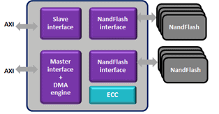
UNFC IP block diagram
The UNFC IP is ONFI 4.2 compliant and supports NV-DDR1, NV-DDR2 and NV-DDR3 modes.
High reliability is provided with this IP thanks to its integrated ECC (Error Correction Code). It is based on a BCH engine. It detects and corrects errors of the data read from the Nandflash memory. Its architecture has been optimized in order to perform this processing at a high rate, without reducing the bandwidth.
Microsemi Polarfire and IP-Maker UNFC, the successful combination
The combination of the IP-Maker UNFC IP and the Polarfire FPGA from Microsemi (a Microchip Company) is an excellent example of reliable integration. This FPGA is well known to be used in safety and mission critical applications. Integrating the nandflash controller in it provides mass storage capabilities, while keeping a high level of reliability thanks to the integrated ECC.
Let’s see how this solution provides benefits at system level. As an example, it can be used as a data recorder, connected to multiple input sources (sensors, cameras…), storing at a fixed frequency the data into the nandflash memory. We assume it is used as a big buffer, and the data are not supposed to be into the nandflash memory for a long time. Then, the data are read, in burst mode, and sent to an end-system. Here, the key challenge is to read a fast amount of data within a very short time.
The way to reach this strong constraint is to increase the total bandwidth. That can be achieved by integrating multiple instances of the UNFC in a FPGA. An important feature when using a nandflash controller in a FPGA (or an ASIC), is the PHY. The PHY is the FPGA part that makes the link between the logical world (the gates array supporting the UNFC IP) and the physical world (connected to the Nandflash memory). According to the Microsemi specifications (from the latest Libero SoC catalog: the Microsemi development tools), the Octal DDR PHY supports up to 200MHz rate. Then, the data bandwidth through a UNFC controller used with this PHY can reach up to 200MB/s per channel, with an 8-bit data bus. This bandwidth can be obtained thanks to the optimized and powerful datapath within the UNFC IP, and thanks to the low latency BCH ECC, able to correct data in few clock cycles.
The total bandwidth is then multiplied according to the number of UNFC IPs used. For example, with 4 IPs (then 8 channels), up to 1.6GB/s can be reached.
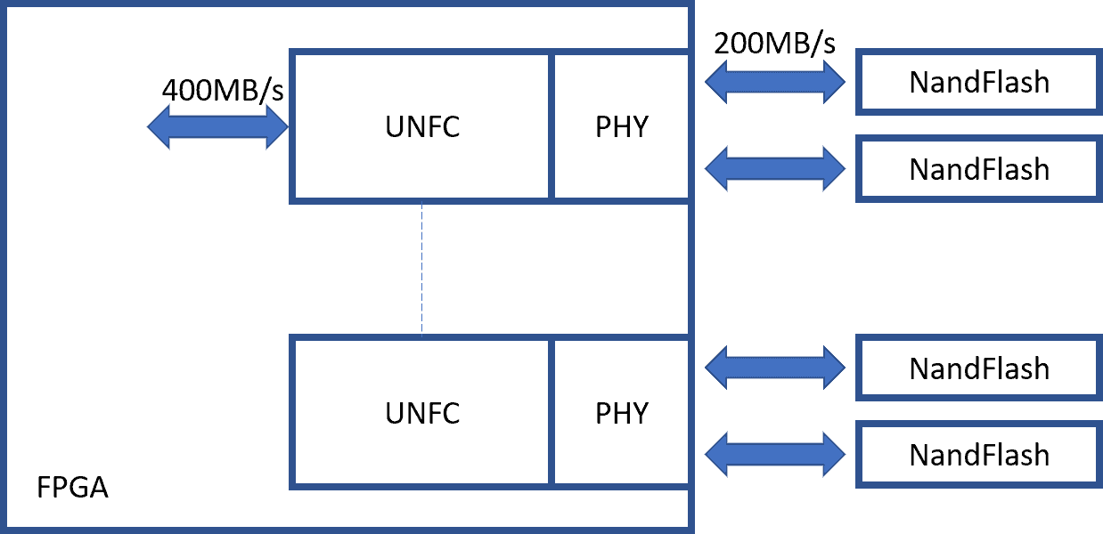
FPGA implementation
Performance, reliability, and low power
Using this UNFC IP in a high reliable FPGA is a perfect solution for safety and mission critical system, including industrial, aerospace and transportation. That combines a high reliability and powerful storage performances. It is fully configurable and customizable at the synthesis stage, reaching the best tradeoff in term of performance and gate count. Last, this overall system, based on low power market winner FPGA and the low gate count, make it ideal for embedded systems with a limited power budget.